- 您现在的位置:买卖IC网 > Sheet目录317 > C8051F380-TB (Silicon Laboratories Inc)DEV KIT FOR C8051F38X
�� �
�
�C8051F380/1/2/3/4/5/6/7/C�
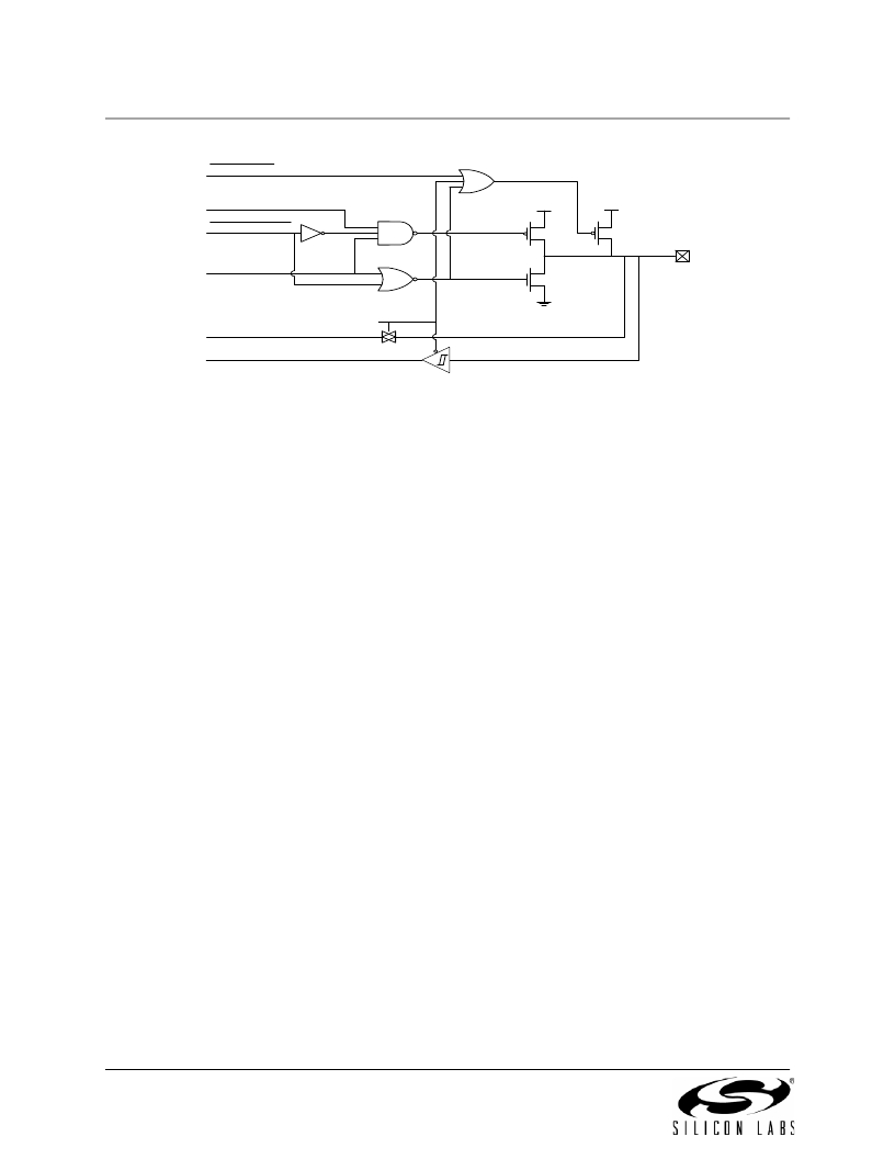
�W� E� A� K� -P� U� LLU� P�
�P� U� S� H� -P� U� LL�
�P� O� R� T� -O� U� T� E� N� A� B� LE�
�VDD�
�VDD�
�(W� E� A� K� )�
�PORT�
�P� O� R� T� -O� U� T� P� U� T�
�A� nalog� S� elect�
�GND�
�PAD�
�A� N� A� LO� G� IN� P� U� T�
�P� O� R� T� -IN� P� U� T�
�Figure� 20.2.� Port� I/O� Cell� Block� Diagram�
�20.1.� Priority� Crossbar� Decoder�
�The� Priority� Crossbar� Decoder� (Figure� 20.3)� assigns� a� priority� to� each� I/O� function,� starting� at� the� top� with�
�UART0.� When� a� digital� resource� is� selected,� the� least-significant� unassigned� Port� pin� is� assigned� to� that�
�resource� (excluding� UART0,� which� is� always� at� pins� 4� and� 5).� If� a� Port� pin� is� assigned,� the� Crossbar� skips�
�that� pin� when� assigning� the� next� selected� resource.� Additionally,� the� Crossbar� will� skip� Port� pins� whose�
�associated� bits� in� the� PnSKIP� registers� are� set.� The� PnSKIP� registers� allow� software� to� skip� Port� pins� that�
�are� to� be� used� for� analog� input,� dedicated� functions,� or� GPIO.�
�If� a� Port� pin� is� claimed� by� a� peripheral� without� use� of� the� Crossbar,� its� corresponding� PnSKIP� bit� should� be�
�set.� This� applies� to� the� VREF� signal,� external� oscillator� pins� (XTAL1,� XTAL2),� the� ADC’s� external� conver-�
�sion� start� signal� (CNVSTR),� EMIF� control� signals,� and� any� selected� ADC� or� Comparator� inputs.� The�
�PnSKIP� registers� may� also� be� used� to� skip� pins� to� be� used� as� GPIO.� The� Crossbar� skips� selected� pins� as�
�if� they� were� already� assigned,� and� moves� to� the� next� unassigned� pin.� Figure� 20.3� shows� all� the� possible�
�pins� available� to� each� peripheral.� Figure� 20.4� shows� an� example� Crossbar� configuration� with� no� Port� pins�
�skipped.� Figure� 20.5� shows� the� same� Crossbar� example� with� pins� P0.2,� P0.3,� and� P1.0� skipped.�
�Registers� XBR0,� XBR1,� and� XBR2� are� used� to� assign� the� digital� I/O� resources� to� the� physical� I/O� Port�
�pins.� Note� that� when� either� SMBus� is� selected,� the� Crossbar� assigns� both� pins� associated� with� the� SMBus�
�(SDA� and� SCL);� when� either� UART� is� selected,� the� Crossbar� assigns� both� pins� associated� with� the� UART�
�(TX� and� RX).� UART0� pin� assignments� are� fixed� for� bootloading� purposes:� UART� TX0� is� always� assigned�
�to� P0.4;� UART� RX0� is� always� assigned� to� P0.5.� Standard� Port� I/Os� appear� contiguously� after� the� prioritized�
�functions� have� been� assigned.�
�Important� Note:� The� SPI� can� be� operated� in� either� 3-wire� or� 4-wire� modes,� depending� on� the� state� of� the�
�NSSMD1-NSSMD0� bits� in� register� SPI0CN.� According� to� the� SPI� mode,� the� NSS� signal� may� or� may� not� be�
�routed� to� a� Port� pin.�
�154�
�Rev.� 1.4�
�发布紧急采购,3分钟左右您将得到回复。
相关PDF资料
C8051F912DK
KIT DEV FOR C8051F91X/C8051F90X
C8051F930-TB
BOARD TARGET/PROTO W/C8051F930
C8051T610DB24
DAUGHTER BOARD T610 24QFN SOCKET
C8051T630DB20
BOARD SOCKET DAUGHTER 20-QFN
CAN-100
BOARD EVAL RS232 100QFP
CANADAPT28
KIT ADAPTER CANDEMOBOARD 28PLCC
CAT24AA01WI-GT3
IC EEPROM SERIAL 1KB I2C 8SOIC
CAT24AA02WI-G
IC EEPROM SERIAL 2KB I2C 8SOIC
相关代理商/技术参数
C8051F381
制造商:SILABS 制造商全称:SILABS 功能描述:USB DRIVER CUSTOMIZATION
C8051F381-GM
功能描述:8位微控制器 -MCU USB-64K-Flash
RoHS:否 制造商:Silicon Labs 核心:8051 处理器系列:C8051F39x 数据总线宽度:8 bit 最大时钟频率:50 MHz 程序存储器大小:16 KB 数据 RAM 大小:1 KB 片上 ADC:Yes 工作电源电压:1.8 V to 3.6 V 工作温度范围:- 40 C to + 105 C 封装 / 箱体:QFN-20 安装风格:SMD/SMT
C8051F381-GMR
功能描述:8位微控制器 -MCU USB-Flash-64k-ADC RoHS:否 制造商:Silicon Labs 核心:8051 处理器系列:C8051F39x 数据总线宽度:8 bit 最大时钟频率:50 MHz 程序存储器大小:16 KB 数据 RAM 大小:1 KB 片上 ADC:Yes 工作电源电压:1.8 V to 3.6 V 工作温度范围:- 40 C to + 105 C 封装 / 箱体:QFN-20 安装风格:SMD/SMT
C8051F381-GQ
功能描述:8位微控制器 -MCU USB-64K-Flash
RoHS:否 制造商:Silicon Labs 核心:8051 处理器系列:C8051F39x 数据总线宽度:8 bit 最大时钟频率:50 MHz 程序存储器大小:16 KB 数据 RAM 大小:1 KB 片上 ADC:Yes 工作电源电压:1.8 V to 3.6 V 工作温度范围:- 40 C to + 105 C 封装 / 箱体:QFN-20 安装风格:SMD/SMT
C8051F381-GQR
功能描述:8位微控制器 -MCU USB-Flash-64k-ADC RoHS:否 制造商:Silicon Labs 核心:8051 处理器系列:C8051F39x 数据总线宽度:8 bit 最大时钟频率:50 MHz 程序存储器大小:16 KB 数据 RAM 大小:1 KB 片上 ADC:Yes 工作电源电压:1.8 V to 3.6 V 工作温度范围:- 40 C to + 105 C 封装 / 箱体:QFN-20 安装风格:SMD/SMT
C8051F382
制造商:SILABS 制造商全称:SILABS 功能描述:USB DRIVER CUSTOMIZATION
C8051F382-GQ
功能描述:8位微控制器 -MCU USB-Flash-32k-ADC
RoHS:否 制造商:Silicon Labs 核心:8051 处理器系列:C8051F39x 数据总线宽度:8 bit 最大时钟频率:50 MHz 程序存储器大小:16 KB 数据 RAM 大小:1 KB 片上 ADC:Yes 工作电源电压:1.8 V to 3.6 V 工作温度范围:- 40 C to + 105 C 封装 / 箱体:QFN-20 安装风格:SMD/SMT
C8051F382-GQR
功能描述:8位微控制器 -MCU USB-Flash-32k-ADC RoHS:否 制造商:Silicon Labs 核心:8051 处理器系列:C8051F39x 数据总线宽度:8 bit 最大时钟频率:50 MHz 程序存储器大小:16 KB 数据 RAM 大小:1 KB 片上 ADC:Yes 工作电源电压:1.8 V to 3.6 V 工作温度范围:- 40 C to + 105 C 封装 / 箱体:QFN-20 安装风格:SMD/SMT